Microwave Integrated Circuits
- 1.1 Classification of Microwave Integrated Circuits
- 1.2 Microwave Circuits in a Communication System
- 1.3 Summary
This chapter is from the book
This chapter is from the book
This chapter is from the book
1.1 Classification of Microwave Integrated Circuits
An active microwave circuit can be defined as a circuit in which active and passive microwave devices such as resistors, capacitors, and inductors are interconnected by transmission lines. At low frequencies, the transmission lines are a simple connection; however, at microwave frequencies they are no longer just simple connections and their operation becomes a complicated distributed circuit element. As a result, a microwave integrated circuit’s classification is based on the fabrication method of the transmission lines used for interconnection.
There are various types of transmission lines in microwave integrated circuits; some common examples are waveguides, coaxial, and microstrip lines. Figure 1.1 shows the transmission lines used in microwave circuits. Although there are special cases of microwave integrated circuits that are composed of coaxial lines and waveguides, in most cases the microwave integrated circuits are formed using planar transmission lines. Therefore, the content of this book is restricted to microwave integrated circuits formed using planar transmission lines, examples of which are microstrip, slot line, and co-planar waveguide (CPW), as shown in Figure 1.2. These planar transmission lines are frequently used in the large-scale production of microwave circuits and generally form the basic transmission lines for microwave circuits.
)
)
Figure 1.1 Some common transmission lines used in microwave circuits: (a) coaxial line, (b) rectangular waveguide, and (c) microstrip line
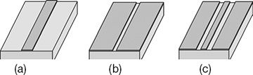
Figure 1.2 Some common planar transmission lines used in microwave circuits: (a) microstrip, (b) slot line, and (c) CPW (co-planar waveguide). They are explained in Chapter 3.
The implementation of planar transmission lines on substrates can be classified into two basic groups: monolithic and hybrid integrated circuits. In monolithic integration, the active and passive devices as well as the planar transmission lines are grown in situ on one planar substrate that is usually made from a semiconductor material called a wafer.
Figure 1.3 shows an example of monolithic integration. Figure 1.3(a) is a photograph of the top side of a wafer and Figure 1.3(b) shows a single monolithic microwave integrated circuit; the identical circuits are repeatedly produced on the wafer in Figure 1.3(a). The monolithic microwave integrated circuit in Figure 1.3(b) is found to contain active and passive devices, and planar transmission lines. The monolithic integration provides a compactsized circuit and eliminates a significant amount of assembly when building a component or a system. Especially because size is of critical importance in most recent RF systems, monolithic integration is frequently employed to provide a compact component. An advantage of monolithic integration is that it is well suited for large-scale production, which results in lower costs. A disadvantage is that monolithic integration takes a long time to develop and fabricate, and small-scale production results in highly prohibitive costs.
)
Figure 1.3 Monolithic integration:(a)a wafer and(b) a monolithic microwave integrated circuit on the wafer (28 GHz GaAs pHEMT Gilbert cell up-converting mixer; refer to Chapter 12).
Hybrid integration is a fabrication method in which the transmission lines are implemented by conductor patterns on a selected substrate with either printing or etching, and active and passive devices are assembled on the patterned substrate by either soldering or wire bonding. When implementing transmission lines by conductor patterns on a substrate, careful consideration must be given to the substrate material and the conductor material for the transmission lines because these materials can have significant effects on the characteristics of transmission lines. Hybrid integration is thus classified into three types based on the method by which the lines are formed on the substrate: a printed circuit board (PCB), a thick-film substrate, and a thin-film substrate.
Figure 1.4 shows an example of how connection lines are formed on a PCB substrate. Both sides of the dielectric material are attached with copper cladding that is then etched to obtain the desired conductor patterns. For PCB substrate materials, epoxy fiberglass (FR4), teflon, and duroid are widely used. FR4 substrate (a kind of epoxy fiberglass) can be used from lower frequencies to approximately 4 GHz, while teflon or duroid can be used up to the millimeter wave frequencies, depending on their formation. Generally, all these materials lend themselves to soldering while wire bonding for an integrated circuit assembly is typically not widely used. Furthermore, compared with other methods that will be explained later, a PCB can result in lower costs; its fabrication is easy and requires less time to produce. In addition, production on a small scale is possible without the use of expensive assembly machines; it is easy to fix and could also be used in large-scale production, and is thus widely used.
)
Figure 1.4 A photograph of epoxy fiberglass PCBs. The PCBs on the left are for the X-band and 2 GHz frequency synthesizers using the phase locked loop. The PCB on the right is for the VHF automatic identification system, which has a similar block diagram shown in Figure 1.7. The power amplifier is implemented in a separate block.
)
Thick-film substrates are produced by screen-printing techniques in which conductor patterns are formed by pushing conductive paste on a ceramic substrate through a patterned screen and then firing printed conductor patterns. The substrate is called thick film because the patterns formed by such techniques are generally much thicker than those formed using thin-film techniques. As a benefit of using screen-printing techniques, multiple screen printings are possible. Dielectric or resistor patterns can also be formed by similar screen-printing techniques using dielectric or resistor pastes. Using an appropriate order of multiple screen printings, it is also possible to form capacitors and resistors on the ceramic substrate. Since the ceramic substrate is more tolerant of heat, it is easy to assemble active devices in the form of chips. On the other hand, considering the lines and patterns formed by this process, the pattern accuracy of thick film is somewhat inferior compared to that of thin film. The costs and development time, on a case-by-case basis, are somewhere between those of the PCB and thin-film processes. Recently, however, the integration based on thick-film technology has become rare because its cost and pattern accuracy are between the PCB and thin-film technology, while thick film is widely used to build multifunction components. A typical example is the package based on LTCC (low-temperature co-fired ceramics) technology.1 Multilayer ceramics and structuring are possible in LTCC technologies. Figure 1.5 shows a photograph of thick-film patterned substrates fabricated using the thick-film process.
)
Figure 1.5 A photograph of substrates fabricated by the thick-film process. Identical circuits can be arrayed for efficient production. This circuit is for the mobile communication VCO presented in Chapter 10.
The thin-film technique is very widely used in the fabrication of microwave circuits for military and microwave communication systems. In the case of the thin-film process, a similar ceramic substrate material used in thick film is employed, but compared to the thick-film substrate, a fine surface-finish substrate is used. The most widely used substrate is 99% alumina (Al2O3). Other substrates such as fused silica, quartz, and so on are possible for conductor-pattern generation based on thin-film technologies. The pattern formation on the substrate is created with a photolithographic process that can produce fine tracks of conductor patterns similar to those in a semiconductor process. Since the thin-film substrate is also alumina as in the case of a thick-film substrate, the assembly of semiconductor chips using wire bonding is possible. Thin film compared with PCB and thick film is more expensive, and due to the requirement of fine tracks, a mask fabrication is necessary and the process generally takes longer. Passive components such as resistors and air-bridge capacitors can be implemented using this process. In addition, integrated circuits produced by the thin-film process require special wire bonders and microwelding equipment for assembly. Compared to the monolithic integration process, the thin-film process tends to be cheaper in terms of cost, but compared to MMIC, the assembled circuit using the thin-film patterned substrate is difficult to characterize precisely because of unknown or poorly described parasitic circuit elements associated with the assembly methods such as wire bonding and die attach. Before the emergence of MMICs (monolithic microwave integrated circuits), thin-film technology was the conventional method for building microwave-integrated circuits (MICs). Figure 1.6 is a photograph of thin-film circuits fabricated with the thin-film technique.
)
Figure 1.6 A photograph of substrates produced by the thin-film process. From top left to bottom right, they are filter, phase shifter, power amplifier (presented in Chapter 9), path-switching circuit by assembly, power divider, and 50 Ω lines.
The choice of integration method depends on the application and situation, taking into account several factors mentioned previously, such as the operating frequency of the integrated circuit, the types of semiconductor components (chip or packaged), the forms of the passive components, large-scale fabrication costs, and method of assembly. These factors should all be considered when selecting the optimum method of integration. For a description of microwave-patterned substrate fabrication, assembly with wire bonding and soldering, and packaging, see reference 1 at the end of this chapter. The book provides general information about microwave-circuit fabrications. Table 1.1 provides a comparison of the hybrid integrations described previously.
Table 1.1 Comparison of hybrid integration
Technology |
Cost |
Fabrication Time |
Pattern Accuracy |
Assembly |
PCB |
Low |
Short |
Low |
Soldering |
Thick film |
Middle |
Middle |
Low |
Soldering and wire bonding |
Thin film |
High |
Long |
Fine |
Soldering and wire bonding |
Now we will consider the application of the planar transmission lines such as microstrip, slot, and CPW to the monolithic and hybrid integration technologies. Microstrip lines are the most widely used transmission lines for both monolithic and hybrid integration technologies. In microstrip lines, the top conductor pattern is usually connected to the ground by a through hole or a via hole. Thus, the back-side process for the through-hole or via-hole fabrication is essential to building a circuit based on microstrip lines. This backside process is inconvenient especially in the monolithic integration. In hybrid integration, the holes can be fabricated through simple mechanical drilling for a PCB case and through laser or ultrasonic drilling for thick- and thin-film cases. Then, plating the fabricated holes completes the fabrication of a through or via hole. However, to fabricate via holes in monolithic integration, a wafer that typically has a normal thickness of about 600 mm should be polished down to about 100 mm thickness. Current technology does not support via-hole fabrication beyond 100 mm. In Figure 1.2, we can see that the CPW and slot lines do not need the back-side metallic ground and they eliminate the need for any additional backside metallization process. The CPW is very helpful in monolithic integration and is widely used to build MMICs without vias. However, the discontinuities of CPWs are not well understood compared to those of microstrip lines and the integration based on a CPW is not as popular as that based on a microstrip. The various discontinuities of microstrip and slot lines, CPWs, and planar transmission lines are covered in reference 2 at the end of this chapter.