- 7.1 Forget the Word Ground
- 7.2 The Signal
- 7.3 Uniform Transmission Lines
- 7.4 The Speed of Electrons in Copper
- 7.5 The Speed of a Signal in a Transmission Line
- 7.6 Spatial Extent of the Leading Edge
- 7.7 “Be the Signal”
- 7.8 The Instantaneous Impedance of a Transmission Line
- 7.9 Characteristic Impedance and Controlled Impedance
- 7.10 Famous Characteristic Impedances
- 7.11 The Impedance of a Transmission Line
- 7.12 Driving a Transmission Line
- 7.13 Return Paths
- 7.14 When Return Paths Switch Reference Planes
- 7.15 A First-Order Model of a Transmission Line
- 7.16 Calculating Characteristic Impedance with Approximations
- 7.17 Calculating the Characteristic Impedance with a 2D Field Solver
- 7.18 An n-Section Lumped-Circuit Model
- 7.19 Frequency Variation of the Characteristic Impedance
- 7.20 The Bottom Line
- End-of-Chapter Review Questions
7.14 When Return Paths Switch Reference Planes
Cables are specifically designed with a return path adjacent to the signal path. This is true for coax and twisted-pair cables. The return path is easy to follow. In planar interconnects in circuit boards, the return paths are usually designed as planes, as in multilayer boards. For a microstrip, there is one plane directly underneath the signal path, and the return current is easy to identify. But what if the plane adjacent to the signal path is not the plane that is being driven? What if the signal is introduced between the signal path and another plane, as shown in Figure 7-21? What will the return path do?

Figure 7-21 Driving a transmission line with the adjacent plane not being the driven return-path plane. What is the return-current distribution?
Current will always distribute so as to minimize the impedance of the signal-return loop. Right at the start of the line, the return path will couple between the bottom plane on layer 3 to the middle plane on layer 2 and then back to the signal path on layer 1.
One way to think about the currents is in the following way: The signal current in the signal path will induce eddy currents in the upper surface of the floating middle plane, and the return current in the bottom plane will induce eddy currents in the underside surface of the middle plane. These induced eddy currents will connect at the edge of the plane where the signal and return currents are being injected in the transmission line. The current flows are diagrammed in Figure 7-22.
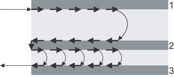
Figure 7-22 Side view of the current flow when driving a transmission line with the adjacent plane not being the driven return-path plane.
The precise current distribution in the planes will be frequency dependent, driven by skin-depth effects. In general, the currents will distribute in each plane to decrease the total loop inductance in the signal-return path. They can only be accurately calculated with a field solver. Figure 7-23 shows an example of the calculated current distribution, viewed from the end, for this sort of configuration for 2-mil-thick conductors at 20 MHz.

Figure 7-23 Current distribution, viewed end on, in the three conductors when the top trace and bottom plane are driven with the middle plane floating. Induced eddy currents are generated in the floating plane. Lighter colors are higher-current density. Calculated with Ansoft’s 2D Extractor.
What input impedance will the driver see when looking into the transmission line between the signal line and the bottom plane? The driver, driving a signal into the signal and return paths with the floating plane between them, will see two transmission lines in series. There will be the transmission line composed of the signal and plane on layer 2 and the transmission line composed of the two planes on layers 2 and 3. This is illustrated in Figure 7-24. The input series impedance the driver will see is:
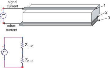
Figure 7-24 Top: Physical configuration of driver driving the transmission line with a floating plane between them. Bottom: Equivalent circuit model showing the impedance the driver sees as the sum of the impedance from the signal to the floating plane and between the two planes.
The smaller the impedance between the two planes, Z2−3, the closer to Z1−2 the driver will see as the impedance looking into this transmission line.
This means that even though the driver is connected to the signal line and the bottom plane, the impedance the driver sees is really dominated by the impedance of the transmission line formed by the signal path and its most adjacent plane. This is true no matter what the voltage of the adjacent plane is. This is a startling result.
The smaller the impedance between the two planes compared to the impedance between the signal and its adjacent plane, the closer the driver will just see the impedance between the signal and floating plane.
The characteristic impedance between two long, wide planes, provided that h << w, can be approximated by:
where:
Z0 = characteristic impedance of the planes
h = dielectric thickness between the planes
w = width of the planes
εr = dielectric constant of the material between the planes
For example, in FR4, for planes that are 2 inches wide with a 10-mil separation, the characteristic impedance a signal will see between the planes is about 377 Ohms × 2 × 0.01/2 = 3.8 Ohms. If the separation were 2 mils, the impedance between the planes would be 377 Ohms × 2 × 0.002/2 = 0.75 Ohm. When the plane-to-plane impedance is much less than 50 Ohms, it is less important which plane is actually DC-connected to the driver and the more likely the most adjacent planes will dominate the impedance.
What if the signal path changes layers in mid-trace? How will the return current follow? Figure 7-25 shows a four-layer board with the signal path starting on layer 1 and transitioning through a via to layer 4. In the first half of the board, the return current must be on the plane directly underneath the signal path, on layer 2. In addition, for sine-wave-frequency components of the current above 10 MHz, the current is actually flowing on the top surface of the layer 2 plane.
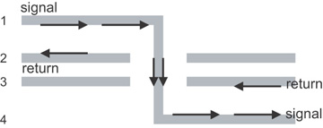
Figure 7-25 Cross section of a four-layer board with signal current transitioning from layer 1 to layer 4 through a via. How does the return current transition from layer 2 to layer 3?
In the bottom half of the board, where the signal is on layer 4, where will the return current be? It has to be on the plane adjacent to the signal layer, or on plane layer 3. And, it will be on the undersurface of the plane. In the regions of uniform transmission line, the return currents are easy to follow. The via is clearly the path the signal current takes to go from layer 1 to layer 4. How does the return current make the transition from layer 2 to layer 3?
If the two planes are at the same potential and have a via shorting them, the return current would take this path of low impedance. There might be a small jog for the return current, but it would be through a short length of plane, and a plane has low total inductance so would not have a large impedance discontinuity. This would be the preferred stack-up. If there were no other constraints such as cost, keeping the nearest reference planes at the same voltage and shorting them together close to the signal via is the optimum design rule. To reduce the voltage drop in the return path, always consider adding a return via adjacent to the signal via.
However, to minimize the total number of layers, it is sometimes necessary to use adjacent return layers with different voltages. If plane 2 is a 5-v plane and plane 3 is a 0-v plane, there would be no DC path between them. How will the return current flow from plane 3 to plane 2?
It can only go through the distributed impedance between them. At the inside of the clearance hole, the return current will snake around and change surfaces on the same plane. The return current will then spread out on the inner surfaces of the planes and couple through the plane-to-plane distributed impedance. The current will spread out between the planes at the speed of light in the dielectric. The current flows in the return path are shown in Figure 7-26. The two return-path planes create a transmission line, and the return current will see an impedance that is the instantaneous impedance of the two planes.
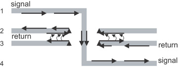
Figure 7-26 The return current transitions from layer 2 to layer 3 by capacitive coupling between the layers.
The return current will have to go through this impedance, and there will be a voltage drop in the return path. We call this voltage drop in the return path ground bounce. The larger the impedance of the return path, the larger the voltage drop, and the larger the ground-bounce noise generated. All other signal lines that are also changing return planes will contribute to this ground-bounce voltage noise and encounter the ground-bounce noise created by the other signals.
As the return current spreads out between the two return-path planes in an ever-expanding circle from the signal via, it will see an ever-decreasing instantaneous impedance. The capacitance per length that the signal sees gets larger as the radius gets larger. This makes the analysis complicated except for specific cases and, in general, requires a field solver.
However, we can build a simple model to estimate the instantaneous impedance between the two planes and to provide insight into how to optimize the design of a stack-up and minimize this form of ground bounce.
To calculate the instantaneous impedance the signal sees as it propagates radially outward between the two planes, we need to calculate the capacitance per length of the radial-transmission line and the speed of the signal. The capacitance per length the signal will see is the change in capacitance per incremental change in radius. The total capacitance the return current sees is:
and the area between the planes is:
Combining these relationships shows the capacitance increasing with distance as:
where:
C = coupling capacitance between the planes
ε0 = permittivity of free space, 0.225 pF/in
εr = dielectric constant of the material between the planes
A = area of overlap of the return current in the planes
h = spacing between the planes
r = increasing radius of the coupling circle, expanding at the speed of light
The incremental increase in capacitance as the radius increases (i.e., the capacitance per length) is:
As expected, as the return current moves farther from the via, the capacitance per length increases. The instantaneous impedance this current will see is:
where:
Z = instantaneous impedance the return current sees between the planes
CL = coupling capacitance per length between the planes
v = speed of light in the dielectric
ε0 = permittivity of free space, 0.225 pF/in
εr = dielectric constant of the material between the planes
h = spacing between the planes
r = increasing radius of the coupling circle, expanding at the speed of light
c = speed of light in a vacuum
For example, if the dielectric thickness between the planes is 10 mils, the impedance the return current will see by the time it is 1 inch away from the via is Z = 60 × 0.01/(1 × 2) = 0.3 Ohm. And, this impedance will get smaller as the return current propagates outward. This says that the farther from the via, the lower the impedance the return current sees, and the lower the ground-bounce voltage will be across this impedance.
We can relate the impedance the return current sees (which is the impedance in series with the signal current) to time since the return current spreads out at the speed of light in the material and r = v × t:
where:
Z = instantaneous impedance the return current sees between the planes, in Ohms
v = speed of light in the dielectric
εr = dielectric constant of the material between the planes
c = speed of light in a vacuum
h = spacing between the planes, in inches
t = time the return current is propagating, in nsec
For example, for a spacing of 0.01 inch, the impedance the return current sees after the first 0.1 nsec is Z = 5 × 0.01/0.1 = 0.5 Ohm. The very first leading edge of the signal will see an initial impedance that can be as large as 0.5 Ohm. If the signal current were 20 mA in the first 100 psec, corresponding to a 1-v signal in a 50-Ohm impedance, the ground-bounce voltage drop across the switching planes that are in series with the signal voltage, for the first 0.1 nsec, would be 20 mA × 0.5 Ohm = 10 mV.
This may not seem like a lot compared to the 1-v signal, but if 10 signals transition simultaneously between the same reference planes, all within less than 0.6 inch of each other, they will each see the same common 0.5-Ohm impedance, and there will be 20 mA × 10 = 200 mA of current through the return-path impedance. This will generate a ground-bounce noise of 200 mA × 0.5 Ohm = 100 mV, which is now 10% of the signal voltage and can be significant. All signal paths that also transition through this path will see the 100 mV of ground-bounce noise, even if they are not switching.
The initial impedance the return current will see can be high, if there is substantial current flowing in a very short time initially. All current flowing during this initial short time will see a high impedance and generate ground-bounce voltages. Figure 7-27 shows the impedance the return current sees over time. From this plot, it is clear that the impedance of the return path is significant only for very fast rise times, substantially less than 0.5 nsec.
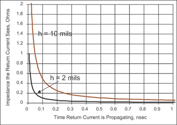
Figure 7-27 The impedance the return current sees between the planes for 2-mil spacing and 10-mil spacing, as the signal propagates outward from the via.
When the impedance is significant—about 5% of 50 Ohms—for one signal line switching, the impedance of the return path is important. When there are n signal paths switching through these planes, the maximum acceptable impedance of the return path is 2.5 Ohms/n.
This is primarily accomplished with the following steps:
Make sure that as the signal path transitions layers, it always has an adjacent plane with the same voltage level for its return and there is a shorting via between the switching planes in close proximity to any signal vias.
Keep the spacing between different DC-voltage-level return planes as thin as possible.
Space out adjacent switching vias so that the return currents do not overlap during the initial transients when the impedance of the return path can be high.
It is sometimes believed that adding a decoupling capacitor between two return planes for which there is a switching return current will help decrease the impedance of the return path. It is hoped that the added discrete capacitor will provide a low-impedance path for the return current to flow from one return plane to the other.
A real capacitor has some loop inductance and some equivalent series resistance associated with it. This will limit the usefulness of discrete decoupling capacitors for very short rise-time signals. The low impedance of the radial transmission line formed by the planes will provide the low impedance for the higher-frequency components.
It is not its capacitance that determines the real capacitor’s impedance above its self-resonant frequency; it is its equivalent series inductance. Figure 7-28 shows the expected impedance of a real 1-nF capacitor with a loop inductance of 0.5 nH. This is an extremely optimistic loop inductance and can be achieved only by either a multiple via in-pad configuration or with the use of interdigitated capacitors (IDCs).
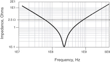
Figure 7-28 Impedance of a capacitor with 1-nF capacitance and only 0.5 nH of loop inductance.
This real capacitor will provide a low impedance for the return path for signal bandwidths only up to 1 GHz. Higher capacitance than 1 nF will provide no added value since the high-frequency components will be sensitive only to the loop inductance.
Unfortunately, even the 0.5 nH of loop inductance of a well-designed capacitor will still have a large impedance at frequencies above 1 GHz, where the planes do not have low impedance and their ground bounce may be a problem.
One additional problem is created when a signal changes return planes and current is driven in the transmission line formed by the two adjacent planes: Where does this current end up? As the current propagates outward, eventually it will hit the edges of the board. The current injected between the planes when the signal current switches will rattle around between the planes, causing transient voltages between the two planes.
The impedance between the planes is very low, much less than 1 Ohm, so the transient voltages created will be low. However, with multiple signals switching between planes, each one injects some noise between the planes. This noise will get larger with more signals switching. The current injected into the planes is determined by the signal voltage and the impedance, roughly 50 Ohms. The voltage noise generated between the planes depends on the signal current and the impedance of the planes. To minimize this rattling voltage, the impedance of the planes should be kept to a minimum by keeping their dielectric spacing thin.
Signals transitioning return planes is a dominant source of high-frequency noise injected between the planes. This voltage noise will rattle around and contribute to the noise in the PDN. In low-noise systems, it can be a major source of cross talk to very sensitive lines, such as rf receivers or analog-to-digital converter inputs or voltage references. To minimize the noise in these systems, care should be taken to minimize the return current injected between the planes by the careful selection of return plane voltages, return vias, and low-inductance decoupling capacitors.
We sometimes call this voltage, which is rattling between the edges of the board between the adjacent plane layers, resonances in the planes. These resonances will eventually die out from conductor and dielectric attenuation. The resonances will have frequency components that match the round-trip time of flight between the board dimensions. For boards with a dimension of 10 to 20 inches on a side, the resonant frequencies will be in the 150-MHz to 300-MHz range. This is why capacitors between the different voltage planes can provide some value. Their low loop inductance provides the low impedance in this frequency regime and helps maintain a low impedance between the planes (in the board resonant-frequency range) and keep the voltages between the planes low. However, as we saw, these capacitors do not affect the transient ground-bounce voltage during the very fast transition.
These problems will get more important as rise times decrease, especially below 100 psec.


